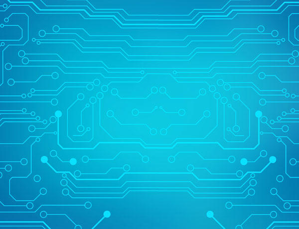
The Importance of Circuit Board Printing:
Circuit boards serve as the backbone of electronic devices, providing the necessary interconnections for electrical signals to flow and components to communicate. By precisely etching conductive pathways onto a non-conductive substrate, circuit board printing facilitates the integration of intricate electrical designs onto compact and durable boards. From smartphones to industrial machinery, circuit boards are omnipresent in modern technology, making their manufacturing process a critical aspect of the electronics industry.
The PCB Manufacturing Process:
Design: Circuit board printing begins with the design phase, where engineers use specialized software to create a blueprint of the desired circuit board layout. This involves selecting appropriate components, defining electrical connections, and optimizing the design for functionality and manufacturability.
Substrate Selection: Once the design is finalized, the appropriate substrate material is chosen. Common options include fiberglass-reinforced epoxy laminates (FR-4) and flexible materials like polyimide. The choice of substrate depends on factors such as board flexibility, thermal resistance, and cost.
Copper Cladding: The chosen substrate is coated with a layer of copper on both sides. This copper layer acts as the conductive material for the circuitry. The copper clad board then undergoes a cleaning process to remove any impurities or oxidation.
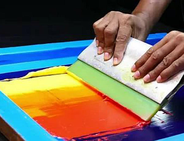
Photolithography: A light-sensitive material called photoresist is applied to the copper-clad board. The circuit board design is then printed onto a transparency film, which is placed on top of the board. Ultraviolet light is passed through the transparency, causing the photoresist to harden in areas not covered by the design.
Etching: After exposure to UV light, the board is submerged in an etching solution that removes the excess copper. The hardened photoresist acts as a protective layer, ensuring that only the desired circuitry remains.
Drilling and Plating: Holes, or vias, are drilled into the board at specific locations to allow for component mounting and interconnection. The holes are then plated with a conductive material such as copper to ensure electrical continuity.
Solder Mask and Silkscreen: A solder mask, typically green in color, is applied to the board to protect the copper traces and prevent solder bridges during assembly. A silkscreen layer is also added for labeling component placements, part numbers, and other relevant information.
Testing and Quality Control: Once the circuit board is complete, it undergoes rigorous testing to ensure its functionality. Automated testing equipment checks for electrical shorts, open circuits, and other potential faults.